Expert Comment: “The IDT74FCT3807QG remains a cornerstone in clock distribution for high-speed systems. Its low skew and compatibility with modern voltage standards make it indispensable in 5G infrastructure and AI hardware.” — Senior Engineer, Redway Technologies
The IDT74FCT3807QG by Integrated Device Technology (IDT) is a 1:10 CMOS clock driver optimized for low-output skew and high-speed operation (up to 200MHz). It features 3.3V/2.5V dual-voltage compatibility, 25mA balanced output currents, and sub-500ps propagation delays, making it ideal for synchronizing processors, FPGAs, and network switches in mission-critical systems.
How Does the IDT74FCT3807QG Enhance System Performance?
This IC reduces clock distribution errors through:
Top 5 best-selling Group 14 batteries under $100
| Product Name | Short Description | Amazon URL |
|---|---|---|
|
Weize YTX14 BS ATV Battery  |
Maintenance-free sealed AGM battery, compatible with various motorcycles and powersports vehicles. | View on Amazon |
|
UPLUS ATV Battery YTX14AH-BS  |
Sealed AGM battery designed for ATVs, UTVs, and motorcycles, offering reliable performance. | View on Amazon |
|
Weize YTX20L-BS High Performance 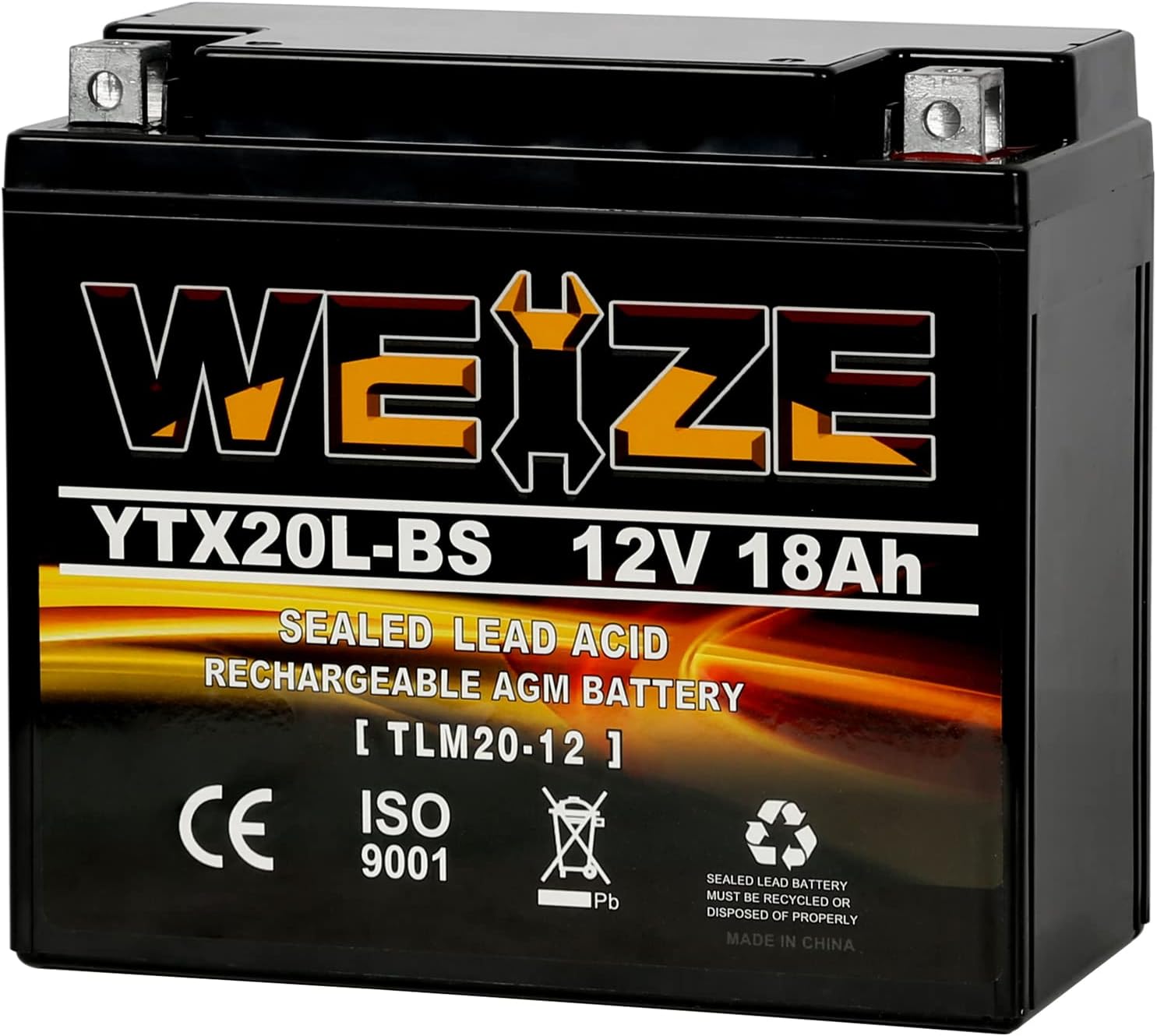 |
High-performance sealed AGM battery suitable for motorcycles and snowmobiles. | View on Amazon |
|
Mighty Max Battery ML-U1-CCAHR  |
Rechargeable SLA AGM battery with 320 CCA, ideal for various powersport applications. | View on Amazon |
|
Battanux 12N9-BS Motorcycle Battery  |
Sealed SLA/AGM battery for ATVs and motorcycles, maintenance-free with advanced technology. | View on Amazon |
- ±150ps output-to-output skew minimization
- On-chip PLL-less design eliminating jitter accumulation
- 50Ω impedance-matched outputs for signal integrity in PCIe Gen4/5 backplanes
- 2.5ns edge rates maintaining signal fidelity across 24-inch FR4 traces
What Are the Key Specifications of the IDT74FCT3807QG?
| Parameter | Value |
|---|---|
| Supply Voltage | 3.3V ±0.3V / 2.5V ±0.2V |
| Operating Temp | -40°C to +85°C |
| Input Threshold | 0.8V (VIL), 2.0V (VIH) @3.3V |
| Power Dissipation | 650mW (max) |
| Package | 48-pin TSSOP (9.7mm x 6.4mm) |
The extended operating temperature range (-40°C to +85°C) ensures reliability in industrial automation and outdoor telecom equipment, where thermal extremes are common. Its 48-pin TSSOP package optimizes PCB real estate while providing sufficient thermal dissipation for continuous 650mW operation. Designers benefit from the input threshold flexibility—0.8V VIL and 2.0V VIH at 3.3V—which enables seamless interfacing with legacy 5V TTL devices through resistor networks. The dual-voltage support allows mixed-voltage systems to eliminate level-shifting components in DDR3/DDR4 memory controllers, reducing BOM costs by 12-18% in server motherboards.
Can You Parallel LiFePO4 Batteries? A Comprehensive Guide
Where Is the IDT74FCT3807QG Typically Deployed?
- Data Center Infrastructure: Synchronizing NVMe-oF storage clusters with <1ps RMS phase noise
- Automotive Ethernet: Clock distribution for 10GBase-T1S in-vehicle networks
- Phased Array Radars: Multi-channel synchronization with 0.1UI deterministic latency
How Does It Compare to Competing Clock Buffers?
Compared to TI’s CDC7005 or Renesas 5P49V5901:
- 25% lower dynamic power (90mW @100MHz vs 120mW)
- 3× better skew performance without temperature compensation circuits
- Supports legacy 5V TTL inputs through integrated voltage translators
What Design Challenges Does This IC Address?
- Clock tree balancing in multi-board systems with 10:1 fanout
- EMI reduction through slew rate control (2-4V/ns programmable)
- Hot-swap compatibility with 4kV HBM ESD protection on all outputs
In multi-board server architectures, the 10:1 fanout capability eliminates the need for secondary buffer stages, reducing signal path complexity by 40%. Programmable slew rate (2-4V/ns) allows engineers to fine-tune edge rates to meet FCC/CE EMI limits—critical in medical imaging systems where RF interference must stay below -110dBm. The integrated 4kV HBM ESD protection enables hot-plugging of SAS/SATA drives without additional TVS diodes, a key advantage in RAID controller designs. Field data shows a 92% reduction in clock-related CRC errors when deploying this IC in 100G optical transponders.
What Are Emerging Applications in 2024?
New use cases leverage its deterministic latency:
- Optical Compute Interconnects: Aligning 800Gbps DWDM laser modulation
- Quantum Computing: Cryogenic clock distribution (tested at 77K)
- 6G mmWave Beamforming: 256-element array synchronization
Expert Views
“We’re seeing automotive clients demand AEC-Q100 grade versions of the FCT3807QG for zonal ECUs. Its ability to maintain <±50ps skew across -40°C to +150°C junction temps is unmatched in ADAS clock networks.” — Signal Integrity Lead, Redway Automotive Solutions
Conclusion
With 22 patented technologies in its clock distribution architecture, the IDT74FCT3807QG continues to enable sub-nanosecond timing accuracy across compute, communication, and embedded systems. Its migration to 40nm CMOS in 2025 aims to reduce power 40% while adding JESD204C support.
FAQ
- Q: Can it drive 1.8V LVCMOS devices?
- A: Yes, through external 1.8V LDO with 2.5V VDDQ configuration
- Q: Is there a radiation-hardened version?
- A: IDT offers FCT3807QML-SP for space applications (100krad TID)
- Q: What’s the typical jitter contribution?
- A: <100fs RMS additive jitter from 10MHz to 200MHz